- 您现在的位置:买卖IC网 > Sheet目录480 > MTD6P10E (ON Semiconductor)MOSFET P-CH 100V 6A DPAK
�� �
�
�MTD6P10E�
�Preferred� Device�
�Power� MOSFET�
�6� Amps,� 100� Volts�
�P� ?� Channel� DPAK�
�This� Power� MOSFET� is� designed� to� withstand� high� energy� in� the�
�avalanche� and� commutation� modes.� The� energy� efficient� design� also�
�offers� a� drain� ?� to� ?� source� diode� with� a� fast� recovery� time.� Designed� for�
�low� voltage,� high� speed� switching� applications� in� power� supplies,�
�http://onsemi.com�
�converters� and� PWM� motor� controls,� these� devices� are� particularly�
�well� suited� for� bridge� circuits� where� diode� speed� and� commutating�
�safe� operating� areas� are� critical� and� offer� additional� safety� margin�
�against� unexpected� voltage� transients.�
�Features�
�V� (BR)DSS�
�100� V�
�R� DS(on)� TYP�
�660� m� W�
�P� ?� Channel�
�D�
�I� D� MAX�
�6.0� A�
�?� Avalanche� Energy� Specified�
�?� Source� ?� to� ?� Drain� Diode� Recovery� Time� Comparable� to� a�
�Discrete� Fast� Recovery� Diode�
�?� Diode� is� Characterized� for� Use� in� Bridge� Circuits�
�?� I� DSS� and� V� DS(on)� Specified� at� Elevated� Temperature�
�?� Pb� ?� Free� Packages� are� Available�
�MAXIMUM� RATINGS� (T� C� =� 25� °� C� unless� otherwise� noted)�
�G�
�S�
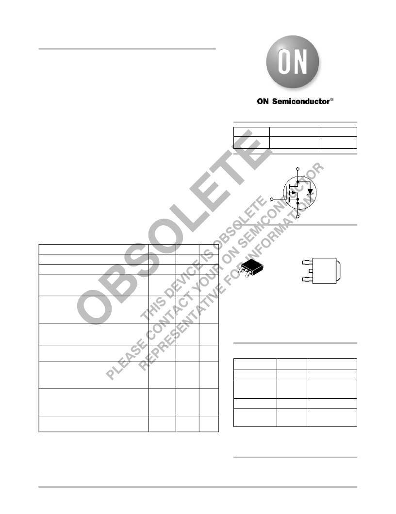
�MARKING� DIAGRAM� &� PIN� ASSIGNMENTS�
�Rating�
�Symbol�
�Value�
�Unit�
�Drain� ?� to� ?� Source� Voltage�
�Drain� ?� to� ?� Gate� Voltage� (R� GS� =� 1.0� M� W� )�
�Gate� ?� to� ?� Source� Voltage�
�?� Continuous�
�?� Non� ?� repetitive� (t� p� ≤� 10� ms)�
�Drain� Current�
�?� Continuous�
�?� Continuous� @� 100� °� C�
�?� Single� Pulse� (t� p� ≤� 10� m� s)�
�V� DSS�
�V� DGR�
�V� GS�
�V� GSM�
�I� D�
�I� D�
�I� DM�
�100�
�100�
�±� 15�
�±� 20�
�6.0�
�3.9�
�18�
�Vdc�
�Vdc�
�Vdc�
�Vpk�
�Adc�
�Apk�
�1� 2�
�3�
�4�
�DPAK�
�CASE� 369C�
�STYLE� 2�
�Y�
�WW�
�Gate� 1�
�Drain� 2�
�Source� 3�
�=� Year�
�=� Work� Week�
�YWW�
�T6�
�P10EG�
�4�
�Drain�
�Total� Power� Dissipation�
�Derate� above� 25� °� C�
�Total� Power� Dissipation� @� T� A� =� 25� °� C� (Note� 2)�
�P� D�
�50�
�0.4�
�1.75�
�W�
�W/� °� C�
�W�
�T6P10E�
�G�
�=� Device� Code�
�=� Pb� ?� Free� Package�
�Operating� and� Storage� Temperature� Range�
�T� J� ,� T� stg�
�?� 55� to�
�150�
�°� C�
�ORDERING� INFORMATION�
�Single� Pulse� Drain� ?� to� ?� Source� Avalanche�
�Energy� ?� Starting� T� J� =� 25� °� C�
�(V� DD� =� 25� Vdc,� V� GS� =� 10� Vdc,�
�I� L� =� 6.0� Apk,� L� =� 10� mH,� R� G� =� 25� W� )�
�Thermal� Resistance�
�?� Junction� ?� to� ?� Case�
�?� Junction� ?� to� ?� Ambient� (Note� 1)�
�?� Junction� ?� to� ?� Ambient� (Note� 2)�
�E� AS�
�R� q� JC�
�R� q� JA�
�R� q� JA�
�180�
�2.50�
�100�
�71.4�
�mJ�
�°� C/W�
�Device�
�MTD6P10E�
�MTD6P10EG�
�MTD6P10ET4�
�MTD6P10ET4G�
�Package�
�DPAK�
�DPAK�
�(Pb� ?� Free)�
�DPAK�
�DPAK�
�Shipping� ?�
�75� Units/Rail�
�75� Units/Rail�
�2500� Tape� &� Reel�
�2500� Tape� &� Reel�
�Maximum� Temperature� for� Soldering� T� L� 260� °� C�
�Purposes,� 1/8� ″� from� case� for� 10� seconds�
�Stresses� exceeding� Maximum� Ratings� may� damage� the� device.� Maximum�
�Ratings� are� stress� ratings� only.� Functional� operation� above� the� Recommended�
�Operating� Conditions� is� not� implied.� Extended� exposure� to� stresses� above� the�
�Recommended� Operating� Conditions� may� affect� device� reliability.�
�1.� When� surface� mounted� to� an� FR4� board� using� the� minimum� recommended�
�pad� size.�
�2.� When� surface� mounted� to� an� FR� ?� 4� board� using� the� 0.5� sq.in.� drain� pad� size.�
�(Pb� ?� Free)�
�?For� information� on� tape� and� reel� specifications,�
�including� part� orientation� and� tape� sizes,� please�
�refer� to� our� Tape� and� Reel� Packaging� Specification�
�Brochure,� BRD8011/D.�
�Preferred� devices� are� recommended� choices� for� future� use�
�and� best� overall� value.�
�?� Semiconductor� Components� Industries,� LLC,� 2006�
�August,� 2006� ?� Rev.� 5�
�1�
�Publication� Order� Number:�
�MTD6P10E/D�
�发布紧急采购,3分钟左右您将得到回复。
相关PDF资料
MTD8000N4-T
PHOTOTRANS 880NM DOME CLR TO-18
MTD8600N-T
PHOTOTRANS 880NM DOME CLR TO-18
MTD8600N4-T
PHOTOTRANS 880NM DOME CLR TO-18
MTD8600T-T
PHOTOTRANS 880NM FLAT CLR TO-18
MTD8600T4-T
PHOTOTRANS 880NM FLAT CLR TO-18
MTE1081C
INFRARED EMITTER 3MM 810NM
MTE2087NJ2
EMITTER IR 870NM DOME CLR TO-46
MTE2087NN
EMITTER IR 870NM DOME CLR TO-46
相关代理商/技术参数
MTD6P10ET4
制造商:ON Semiconductor 功能描述:Trans MOSFET P-CH 100V 6A 3-Pin(2+Tab) DPAK T/R
MTD7030
制造商:MARKTECH 制造商全称:Marktech Corporate 功能描述:PHOTO DIODE
MTD7030A
制造商:MARKTECH 制造商全称:Marktech Corporate 功能描述:PHOTO DIODE
MTD8000M3B-T
制造商:Marktech Optoelectronics 功能描述:PHOTOTRANS 880NM DOME 3MM
MTD8000M3B-T-DIG
制造商:Marktech Optoelectronics 功能描述:PHOTOTRANS 880NM DOME 3MM
MTD8000N
制造商:MARKTECH 制造商全称:Marktech Corporate 功能描述:Metal Can Photo Transistor
MTD8000N_2
制造商:MARKTECH 制造商全称:Marktech Corporate 功能描述:Optical Switches, Edge Sensing
MTD8000N4T
制造商:MARKTECH 制造商全称:Marktech Corporate 功能描述:Peak Sensitivity Wavelength: 880nm